(This is the translation of the original article performed by baragol)
We had a bunch of photographs of the main PCB, a YouTube video with drain-voltage waveforms of MOSFETs, a forum post with a breakdown of the capacitance values of LC circuit capacitors and also a number of unboxing videos showing the heating-up of the soldering tip. The only thing that really worried me was the video with the measurement of the peak power consumption during the heating-up. There is nothing in the world more helpless and irresponsible and depraved than burned cartridge newly bought for 60 bucks from Amazon. But let me start from the beginning.
Introduction into the subject matter
To understand what kind of device we are going to design today, let’s first have a brief recollection of the kinds of soldering stations on offer and how they are different.
As you might have guessed, the entire low-end price segment of this equipment is possessed by Chinese brands, which largely clone the fairly successful design of the Japanese soldering iron Hakko. The operating principle behind both the original model and its numerous replicas is very straightforward: a nichrome or thin-filmed heater transfers its heat to a detachable soldering tip, its temperature being regulated with a thermocouple unit or a thermistor built into the heater. This is a plain and cheap solution, but its quality may turn out slightly far from perfect in Chinese replicas, e.g. a slightly wrong-sized heater, a slightly cheaper material of the tip, which all result in having to wrap the heater in foil, ordering an original Japanese tip from abroad, replacing the connector with a more powerful one… in other words, you’ll have your plate full in no time.
Somewhere in the middle on the price spectrum are the original soldering stations from renowned western brands. The German ERSA, the U.S. Weller, the Japanese Hakko – that sort of brands. Their operating principle is basically identical, except that you don’t really need to get to your resources to make them work; they include nice out-of-box goodies, such as a soft silicon cable that does not melt from at slightest touch of the soldering iron, and… well, there aren’t that many goodies actually! The price? Matches the promise. The hundreds of bucks to spend on the stuff can distress not only a humble DIY enthusiast who is fond of spending his evenings tweaking his hardware, but even a mid-scale business.
However, today’s article is about something different. I will tell you about the real high-end phenomenon in the world of soldering stations, namely the made-in-the-U.S.A. induction soldering irons from Metcal (they are currently produced under this brand by OK International). Actually, several companies are producing these pieces of equipment, e.g. apart from Metcal, I can also mention Thermaltronics, JBC, and even Hakko who sell a similar design. The operating design of the induction heater in these devices is quite elegant:
As you can see, it lacks any temperature sensors whatsoever; its soldering tip is made of copper with a ferromagnetic coating, which, when exposed to a high-frequency (13.56 MHz) alternating magnetic field, gets heated and then, at a certain temperature, called the Curie temperature, loses its magnetic qualities and stops heating up any further. When you touch the soldering point, the ferromagnetic item partially loses its heat, and the inductor immediately starts transmitting its power to the soldering tip. The cartridges come with four fixed temperatures, of which you really need only two – for lead and lead-free soldering. That’s all it is.
OKI/Metcal produce several models of induction soldering stations that come at different prices and with different output power, however, the price range of $1000 rids one of any desire to take advantage of this beautiful device, no matter how beautiful it may seem. Which brings me to the idea of trying to save some money!
Problem
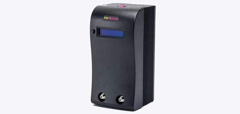
Let’s put it like this: by using only publicly available sources, to undertake the virtual reverse engineering of the original device MX-5200 and end up with the design of a consumer-class single-channel high-frequency waveform oscillator with the output power of 80W, which will replicate the functionality of the original soldering station as much as possible.
If you do some online searching, you will easily find a schematic diagram of the previous generation of Metcal MX-500 station, carefully copied from its PCB. The direct implementation of the design ideas from that diagram won’t work as the output power of this piece of equipment is just 40W, and it can’t be easily scaled up. However, this old diagram will help us understand the operation of the key assemblies.
So, the following elements can be seen in the diagram:
- A high-power HF generator with three output resonant circuits;
- A pulse step-down converter for powering the generator (1), with the output voltage ranging 17-21V;
- A feedback circuit to regulate the voltage of the step-down converter (2) depending on the voltage on one of the output resonant circuits of the generator (1);
- A protection circuit to switch off the generator (1) in case of the disconnection of the inductor;
- A transformer power supply unit with the output voltage of 53V.
Let’s quickly consider some common circuit design solutions. For example, the circuit can be powered with a low-frequency toroidal core transformer. Hold on, let’s rather use a resonant LLC transformer with a rare microchip HiperLCS from Power Integrations: I’ve long been meaning to work with it. Let’s also take a more up-to-date step-down transformer to control the output power and see if we can possibly get 5A out of a SO-8 package. Wait a minute, can a project survive without an Arduino, a sketch, and a LED? Let’s also add a STM32 chip and a small display for showing the current output power. To make things simple, we’ll measure the power in the HF generator power circuit; as for efficiency, we’ll take it into account (or shall we ignore it) in the software. We’ll use a metal case of the right size, which will serve both as a shield and a heatsink at the same time.
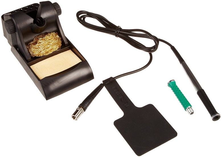
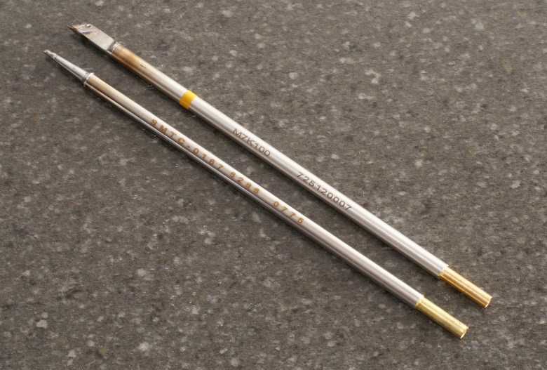
For the actual soldering, I’ll go to Amazon and purchase a Metcal MX-UK1 upgrade kit, including a workstand and the soldering iron itself (which is just a hand-piece attached to a wire), and soldering cartridges. Based on my work experience, I find it easier to handle small items with a 30° hoof soldering iron tip, and for soldering anything bigger I’ll take something wider, heavier and hotter, so here’s my choice: a Metcal SMTC-0167 for fine soldering and a Thermaltronics M7K100 for working with larger scale items. By the way, cheaper Thermaltronics tips will also do the trick.
While my items are being shipped, I’ll draw a flow diagram of the device in project.
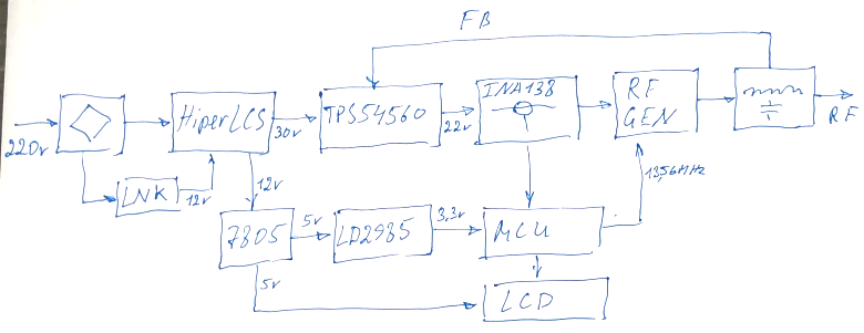
It is important to outline the feedback between the output of the HF generator and the control input of the step-down converter. The thing is, after a soldering tip has been heated to the operating temperature, the oscillator keeps outputting a fairly high amplitude voltage (around 100V), and the resulting power starts dissipating on the active resistance of the inductor coil, which, due to the skin effect, is much higher than an ordinary multimeter can register. As a result, the tiny coil grows red-hot and burns off. To prevent this, the original stations use a negative feedback that reduces the power-supply voltage of the oscillator in response to the growing standing-wave ratio that comes with the change in the impedance of the inductor. The 40W model uses a relatively straightforward method from the US4626767A patent, whereas the 80W model uses a more sophisticated feedback involving a current transformer. Let’s take a look at this video which you can find on the web:
The blue line shows the supply voltage on the output stage of the HF generator, and as you can see from the video, we need to provide for the supply voltage to be able to increase by at least double (accordingly, the output power will be growing in proportion to the voltage squared, i.e. four times the voltage value). Since I did not succeed in ensuring the same quality of regulation with a simple feedback circuit I modelled in LTSpice, I just copied the feedback circuit from the photograph of the PCB.
High Frequency Generator
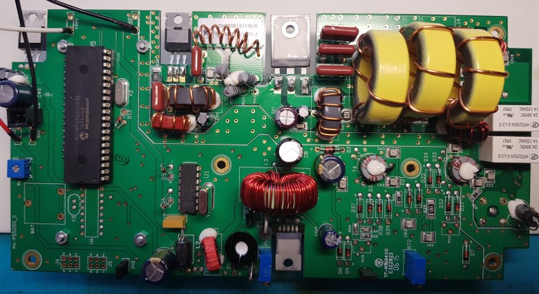
Let’s start designing the high-frequency module by first working out the output resonant circuit. Take a look at this high-resolution photo:
You can see three coils wound around yellow toroidal cores, with 4, 6 and 7 turns respectively, from left to right. By Amidon’s classification system, yellow is used for powdered-iron cores with the permeability of 8.5 (material #6). The size of the coils can be calculated by first using a ruler to measure the diameter of the coils on the screen and then comparing that against the measure of some well-recognizable component, such as the output transistor in the TO-247 package. Apparently, this design uses T130-6 cores; this, in my opinion, is a bit of an overkill – such large toroids are intended for a much higher power. But I have no intention to play smarty pants here: I certainly can’t afford the original U.S. cores, so instead I will order their cheap Chinese replicas from AliExpress and see if they can do the job (spoiler alert: they did just fine). Their inductance values were calculated as 180, 400 and 540 nH respectively.
In the resonant circuits, inductors operate alongside capacitors. We can’t derive their capacitance values from the photograph, however we can easily find a message post by the punctilious mikeselectricstuff (the author of the video above) who kindly shared his observations (highlighted in yellow):
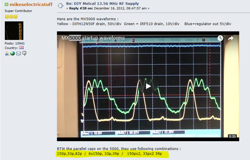
After feeding these values to a spice model, it becomes clear that the resonant frequencies of the circuits are slightly shifted away from 13.56 MHz. The thing is, the closer the frequency to the self-resonant one, the less voltage is needed to power the HF generator and the higher is its current consumption. The original design powers the output stage with a step-down converter with a 3A current limit, so the designers put the output stages slightly out of resonance to be able to increase the supply voltage and decrease the usage of current. We, on the other hand, are planning on employing a 5A chip, however, it turned out to be short of current while in resonant mode, so we’ll similarly put the output stages out of resonance just a little bit. We’ll find out the exact capacitance values experimentally, based on the project limits for the maximum supply voltage of the output circuit (22V) and the maximum usage of current (4A).
Note that quite an amount of energy flows within the resonant circuits, eager to be released into the environment in the form of heat. So to increase the Q-factor, let’s use fairly thick enameled wire (1.25mm) for the coils and connect several capacitors in parallel.
Choosing the right output transistor is another puzzling question. In case the cartridge is replaced or removed, the overvoltage can surge to 300-350V, but the authors of the original design chose not to bother with sophisticated protection and simply equipped the output stage with a pretty rare, fast and expensive RF transistor IXFH12N50F from IXYS with the drain voltage limit of 500V. We can’t afford such luxury, so let’s take a standard 200V field-effect transistor STP19NF20 that costs just half dollar and connect it in parallel with a 150V surge suppressor. Perfect! The suppressor will slightly cut off the surges of the resonant circuits, keeping them from swinging too much, while the protection module will halt the oscillator within around 10ms after the load disappears.
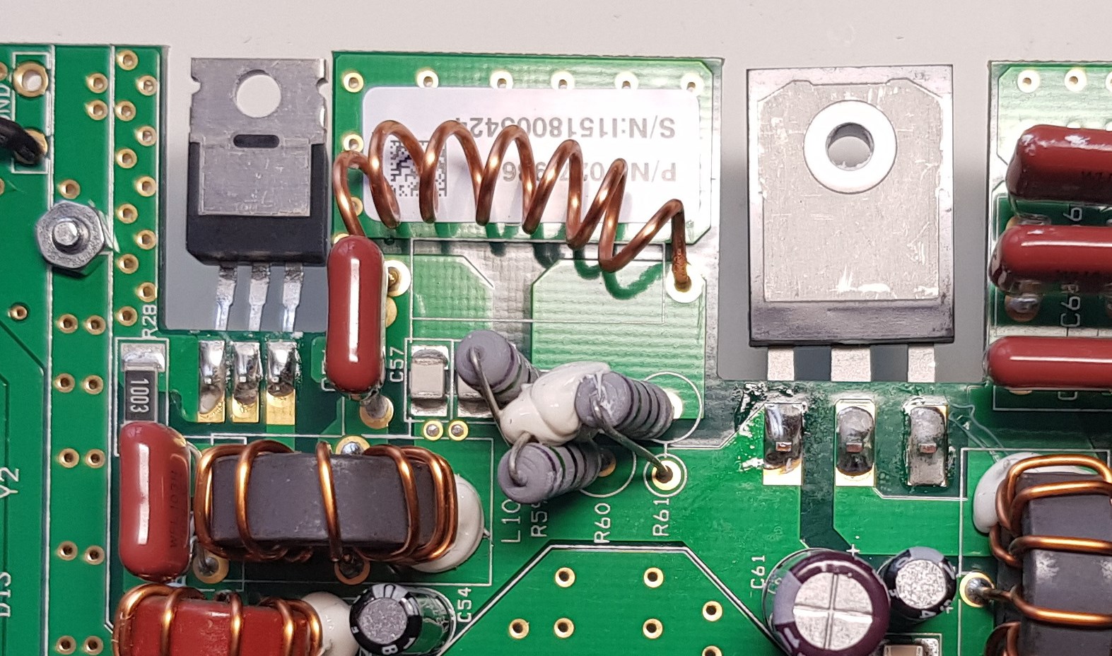
Because of the large input capacitance and high frequency, we can’t control the gate of the output transistor directly with a usual gate driver. The photo of the original board reveals a coreless inductor coil between the two power transistors. This is a commonly used little trick: together with the gate-source capacitance, the inductor creates a resonant circuit that sustains the energy flow across the gate circuit, which results in a surge in the efficiency of the pre-amplifier. At the same time, that same circuit imposes an implicit restriction on the possible model of the output transistor: its gate resistor value must be as low as possible to maintain a reasonable Q-factor of the circuit. Without going into much details, let’s reproduce the manufacturer’s solution. We’ll select the right inductance value based on the maximum efficiency of the actual circuit by tightening/stretching the windings of the coil.
From then on, the circuit design grows more trivial. We will be driving the pre-amplifier designed around an IRF510 transistor with low input capacitance using a dual driver MAX17602, as its speed characteristics look good. A MAX17600 or a MAX17601 would work even better, and we could connect their outputs in parallel, but I did not have those immediately available, so we’ll work with whatever we have.
The correct oscillating frequency will be set by a crystal resonator. Unfortunately, I couldn’t find a 13.56 MHz crystal for the active oscillator. But no worries, we’ll take a more commonly used 27.12 MHz resonator and halve the frequency. We’ll make good use of a microcontroller, or rather one of its timers programmed accordingly. I should also mention that an MCU can only be directly connected to a crystal resonator working at the fundamental frequency of the crystal. The commonly used Russian third-overtone 27,120 kHz resonators can only be connected through a quick hack in the form of an extra resonant circuit.
Power supply
After a long series of fruitless experiments with products made in China, I decided to power the output stage of the HF oscillator from a step-down converter based on TI’s TPS54560 chip. To prevent any audible beats, we will set the internal oscillator frequency at around 450 kHz, at a distance from the working frequency range of the LLC converter. Alternatively, I could have done just the opposite, i.e. sync the step-down converter with the oscillator of the LLC converter, but at that point I was getting lazy, so I dropped this idea.
The TPS54560 converter itself, despite its tiny size, boasts a considerable output current value, so at times you could imagine this is some unprecedented advance in a struggle for energy efficiency… Yet the truth is, the chip really does need to be properly cooled down. The demo board offered by Texas Instruments contains two large ground planes 2oz thick on both sides; the heat transfer across the layers is ensured by six via holes just beneath the chip bottom (where it has a heat dissipation pin). Such layout makes it somewhat harder to make a DIY board, so I’ll obviously have to order it from a Chinese manufacturer. Bugger!
To power the driver and pre-amplifier, let’s take the 12V unregulated voltage off the second coil of the LLC converter. The current drain on the rest of the board will be negligible, so to power the 5V controller and to light up the LCD display, we’ll use the domestically produced linear regulator KR142EN5A, whereas the 3.3V line for the MCU will be regulated by the miniscule LD2985.
To reduce line voltage down to the required 30V and 12V, we’ll employ an LLC converter based on the LCS708HG chip.
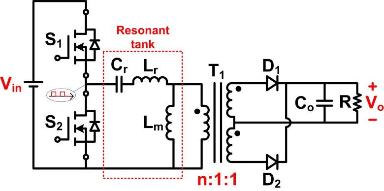
I’m sure many readers would like to know more about LLC converters, so I’ll explain its operating principle in more details. The LLC is not quite an acronym, as these letters stand for “inductor-inductor-capacitor” and, in short, implement the electrical design for connecting the primary winding of a transformer. The point is, sometimes some part of the flux generated by the primary winding may not link to the secondary winding, which causes so-called leakage inductance – stray inductance that is unable to transfer the accumulated energy to the secondary circuit. In standard flyback converters, this energy has to be dissipated on suppressors or snubber resistors, so transformers (or, more specifically, double-coil chokes) are usually designed in such a way as to reduce the leakage inductance as much as possible. Yet things are completely different with LLCs.
In a resonant converter, the leakage inductance combined with the capacitance connected serially to the primary winding create a tank circuit which solves two important problems. First, it does the switching of the output high-voltage transistors of the converter at close-to-zero voltage values (the so-called Zero Voltage Switching, ZVS), which significantly cuts down energy losses caused by the switching. Second, the energy accumulated in the uncoupled inductor flows back into the circuit, so this removes any need in snubbers as there is actually no energy loss. In its application note AN-55, Power Integrations provides a detailed outline of how to a design a transformer to increase its leakage inductance (this is needed to ensure the right transformer characteristic). I, for example, wound primary and secondary turns wide apart, in two different sections:
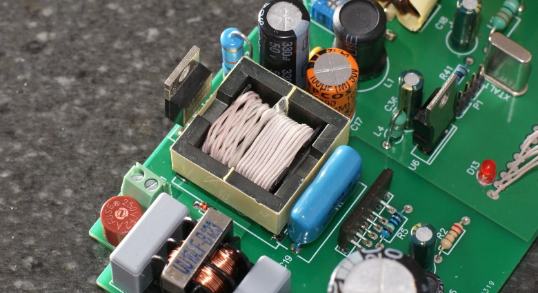
Generally, such fancy layout design results in a very decent efficiency value, e.g. an LCS708HG chip without a heatsink, despite its miniature size, delivers the output power of about 200W! This is a truly outstanding result, but you can only achieve it when operating at exactly the self-resonant frequency of the output circuit. This is where the catch is.
The thing is, in this case, the output voltage is regulated by changing the pulse frequency rather than the pulse ratio, and the regulation takes place in a very narrow range of voltage – around ±15%. Besides, in response to the fluctuations of the input voltage from its nominal value, the conversion frequency shifts away from resonance, imposing the hard-switching mode on the transistors inside the chip, consequently heating them up a lot. In effect, the converter needs to receive regulated voltage on its input!
In factory-made products, converters are equipped with active power factor correctors (APFCs) at their input, which, apart from actually correcting power, also maintain an output voltage of around 380-390V. But after all, we are dealing with a DIY design here, so let’s blissfully ignore such trifle hiccup as the sensitivity to the quality of line power. Based on the calculations and with allowance for voltage pulsation on buffer capacitance, the input voltage is in the range of approximately 230V ± 10%, so if the power grid operates within the standards, everything is going to work smoothly. Let’s leave it at there for now.
We’ll copy the rest of the converter design from the relevant datasheet. I’d probably only focus on the resonant capacitor – this apparently straightforward component. If you ever wondered what the difference is between Polypropylene film capacitors and Polyethylene Terephthalate (PET) film capacitors, here is the answer: the former ones have a ten times smaller loss tangent. That’s precisely why my attempt to replace the bulky K78-2 (another domestically produced product) with a cheaper and smaller PET model K73-17 caused some curious behavior: the capacitor went into an overheat and began generating suspicious crackling noise. Interesting.
The chips of the HiperLCS series require a dedicated 12V power supply line. To save the trouble of fiddling with an additional winding, a rectifier and startup circuits, let’s stick to the textbook. We’ll obtain the required voltage from a separate tiny converter on a LNK304 chip. Its key feature is its transformer-free design, as the only inductor we’ll need is a cheap factory-made choke. The maximum output current remains within a small range, about 100mA, and the simplicity of the design along with the ability to keep the number of components to a minimum make it an attractive solution (whereas the number of converters per square inch of surface is starting to get on my nerves. The God of converters demands more of them!)
Brain
Well, just a few more things to do. The original station has an LCD which, for the price you’ve paid, displays a resemblance of the output power. Let’s do something similar: we’ll take the STM32F030 controller in its minimum configuration (in a TSSOP-20 package). One of the inputs of the A/D converter will measure the supply voltage of the output stage in the HF generator, while the other input will measure the current. To avoid breaking the ground circuit, we’ll attach the current sensing resistor to the positive wire and implement level shifting using the special-purpose INA138 chip, a design of Burr-Brown in its glorious days. To display information, let’s use a text OLED with a 16x2 resolution made by WinStar. That’s it in a nutshell. Wait, we have left one processor pin unoccupied. Well, let it blink a LED then. Don’t ask me why.
The controller firmware was written in C language using STM32CubeMX and the free version of IAR Embedded Workbench. The code is quite trivial. At the tick of the system timer, once in 300ms, the main loop reads data from the two channels of the A/D converter, multiplies them and sends to the display as the power reading. In the bottom of the screen, the power value gets visualized in a bar rendered with customized fonts. Upon the switching-off of the soldering tip, the handler of the interrupt coming from the output of the load detector stops the reference timer of the HF oscillator. To insure against any freezing or fault in the MCU, I have added handlers for hardware errors and the watchdog timer signals; the firmware also employs the CSS (Clock Security System) technology that, in case of a damp in the oscillations of the primary crystal resonator, switches to the built-in RC oscillator and relaunches the microcontroller. The total size of the firmware is 10 KB. I uploaded the source code of the firmware together with the other project files to GitHub for the most curious of you to take a look (but don’t expect anything extraordinary there).
Layout
- MOSFET drain chokes and the current transformer was wounded on a HF-ferrite 16x8x6mm ring cores with permeability of 50. It’s ok to use 0.6mm enameled wire, chokes have 15 turns, current transformer — 2x14 turns;
- Coreless inductor has 10 turns of 0.6mm wire uniformly distributed along 10mm length. The inner diameter is 5mm;
- The main transformer is based on a small EFD25 core of N87 Epcos material. I’ve added a 0.2mm gap on the each leg by inserting of two layers of note paper. That gives us a 0.4mm gap in total. For the primary winding (33 turns) and the first secondary winding (2x6 turns) the triple insulated litz wire is used with size of 100/46 and 175/46 respectively (here the first number is the wire count, and the second one is the AWG diameter). Second secondary 10V winding has two turns of any appropriate flexible stranded wire (I’ve used PTFE-insulated one).
The calculations for all the components of the LLC converter, including the inductance values of the transformer windings, are provided in the layout file attached to the project, which you can view using PI Xls Designer. I also included all the datasheets for the electronic parts I used in the project, uploaded LTspice models of some parts of the circuit and a few photos of course.
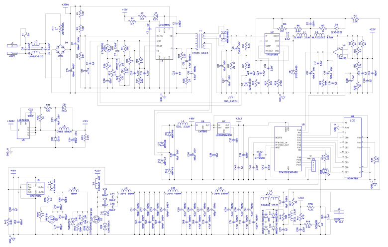
The result of the design described above is the following electric schematic diagram:
The diagram and PCB layout were prepared using DipTrace, with the drawings converted to the Gerber format for further dispatch to the manufacturing plant. The PCB layout is made to fit closely into the device case, with one entire layer covered with a ground plane to shield fragile low-current circuitry. Such layout makes it much easier to manufacture the board at home, as it does not require any precise alignment of photo templates: you can fill almost the entire reverse surface of the board with one solid plane and then use a thick drill to make hole bevels around those pins that do not need to be grounded.
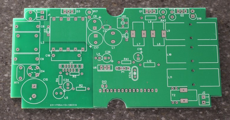
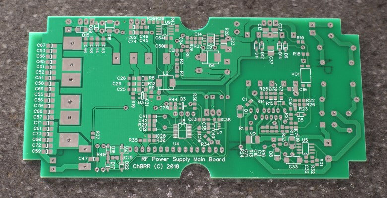
Since some HF parts used in the design emit much radio-noise and the power components are easily overheated, naturally my choice of the material for the case will be aluminum. I’m going to pick an approximately matching case G0476 from Gainta’s catalog. We will cut out a window in the case for the OLED using a rotary tool. We will then connect the case directly to the earth wire of the power cable together with the shield of the solder cable and the PCB ground.
Unfortunately, the idea of connecting a more contrast OLED instead of an LCD came to me well after I had sent my PCB order to the manufacturing plant. The input CMOS levels of an WEH001602AGPP5N00001 OLED from WinStar are different from the standard TTL levels of an LCD, so the trick with feeding +5V to the display controller and its lighting, and then reading the logic signals from the microprocessor powered from +3.3V won’t work here. I had to connect the display to a 3.3V line using a separate wire.
To reduce noise, I installed 390 Ohm interference-suppressing resistors into the bus connecting the PCB and the display, and covered the microcontroller with a copper foil shield. Under normal operation, the programming connector must be covered with a female part that grounds the debug pins directly and the NRST pin – via a capacitor.
In the end, my device acquired its final appearance:
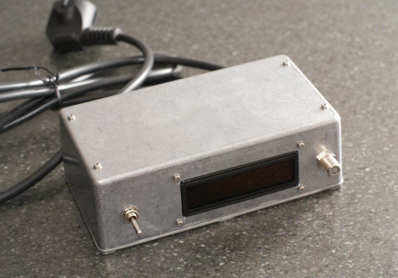
Here is the resulting procedure for the heating-up of the soldering iron:
Bottom line
Now let’s total up the spending on this little piece of fun:
Electronic components – about $50 (the most expensive ones were the HiperLCS chip for $15 and the OLED for $10);
PCB fabrication, cost per 10 pcs. – slightly over $40;
Case – $8.
The total cost of the actual high-frequency power supply unit came at around $100. I have also paid for a soldering iron with a workstand ($170) and two cartridges ($100).
I could of course optimize the spending to some extent, for example eBay has a broad range of used Metcal parts, in this case we’re talking about just a few tens of bucks, but that’s probably a matter of personal preference.
Errata
- Crystal load capacitor network was routed in a wrong way and is very sensitive to HF noise. The right way is that. Thanks to Alexander Chulkin for this important enhancement.
- There is no support for the ability to disconnect the cable of the soldering iron from an operating station, as sometimes it may restart the microcontroller. It’s worth considering the introduction of some additional shielding of the HF part (I’m not 100% sure though).
Conclusions
Now let me share with you the ultimate goal I was pursuing with this project – the experience I get from working with the device. It feels like using a very powerful and red-hot soldering iron while holding a small and light tool in your hands. Whether it was worth the money and effort spent, it’s hard to say. I’ll leave the question open.

Автор: SergeyMax


